


What is the general process for designing an FPCB in Consilia?
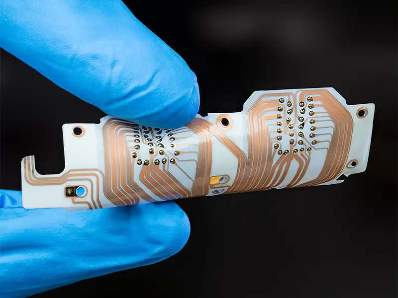
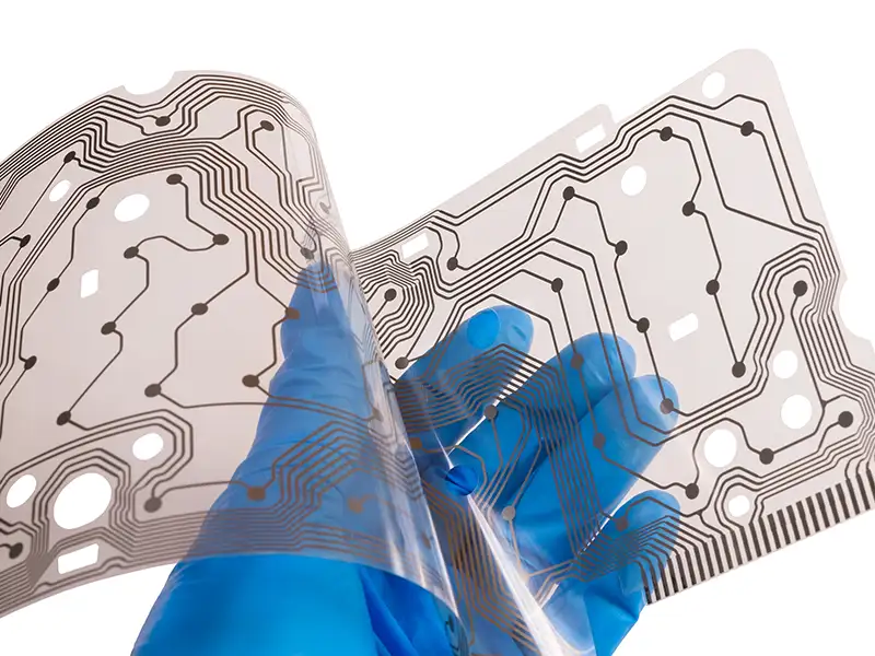
In general, the FPCB design process follows many of the same principles as traditional rigid PCB design. The process begins with defining the mechanical outline, including mounting methods and height constraints, in cooperation with the mechanical engineering team. Within these boundaries, the component layout and FPCB stackup are developed to meet the requirements of electrical hardware engineers and applicable standards such as EMC. Finally, the design is connected, traced, and prepared for manufacturing, including all necessary production data and documentation.
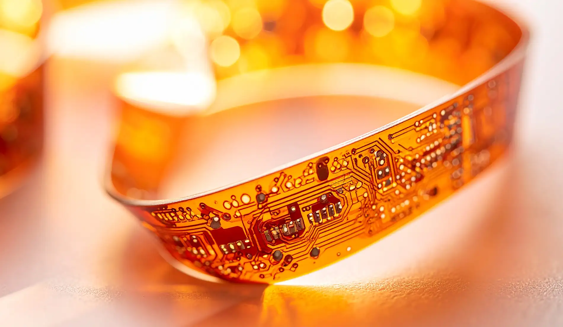
However, for FPCBs, each of these steps is more specific and more complex. Although FPCBs are significantly thinner, their ability to bend and fold introduces new opportunities in three-dimensional applications, requiring closer coordination with mechanical engineering. Routing on FPCBs also differs from rigid PCB design, as it requires rounded traces and mesh structures, which add time and complexity.
The key difference lies in the stronger interconnection between the rules governing each discipline and the deeper interdependencies across the design process. As a result, FPCBs demand more communication and closer interdisciplinary collaboration.
Designing an FPCB comes with complexities and considerations not found in the rigid PCB design process. What are some of the key differences?
If you reach a point in your PCB design where additional layers are required, the change is typically straightforward. Manufacturers can often add two layers using thinner dielectrics without altering the overall board thickness. If that isn’t possible, the thickness increases by about 10%, with a similar rise in cost. In most cases, the mechanical impact is minimal and may even provide a slight increase in strength.
In FPCB design, however, the same situation has far more significant consequences. Adding layers results in a substantial increase in thickness, greatly reduced flexibility, and a dramatic increase in minimum bend radius. These changes can strongly affect the device’s overall mechanics, leading to increased redesign time and higher development and production costs. Thin shielding layers present similar challenges from an electrical design perspective.
FPCBs can sometimes suffer from strain on their components from over flexing, or from signal integrity issues from electro-magnetic interference. What can you do in the design phase to reduce those risks?
These are all important considerations, and we address them from the very beginning of the design process across all teams. Mechanical engineers apply additional reinforcement, protective layers, or sliding foils in critical areas. Similar measures are taken on the electrical side, such as specifying shielding foils for EMC and EMI protection. However, the most influential factor is the total length of the wiring. Efforts to minimize this length often determine whether FPCBs can be used in compact or miniature devices.
Despite their advantages, FPCBs are not appropriate for all applications. Can you give an example of a project where an FPCB was required and why?
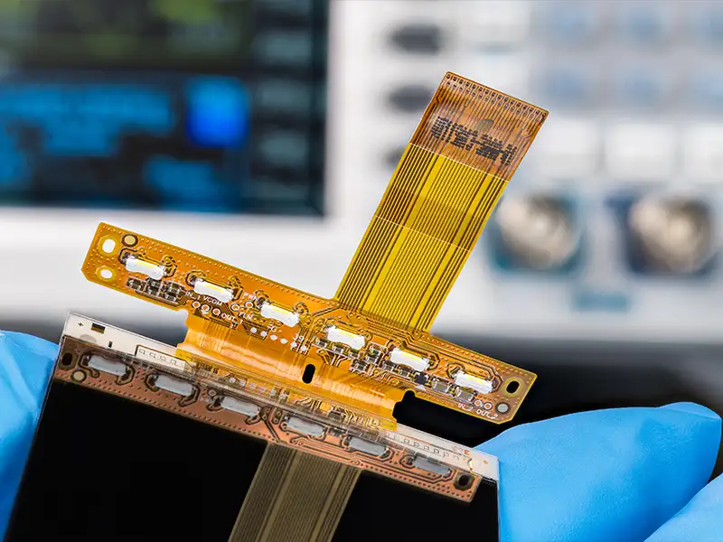
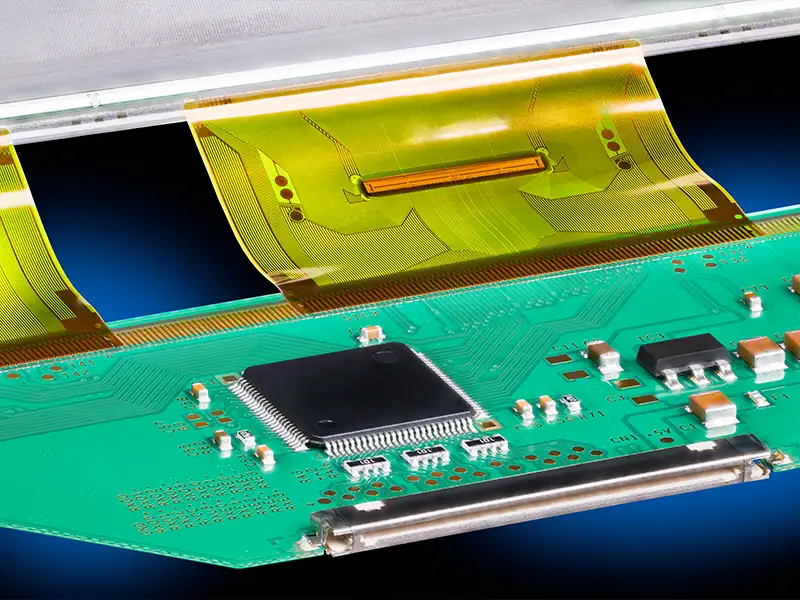
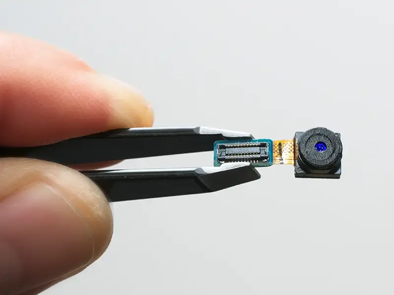
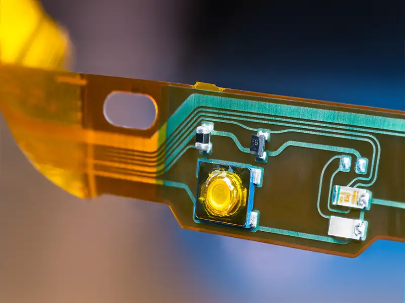
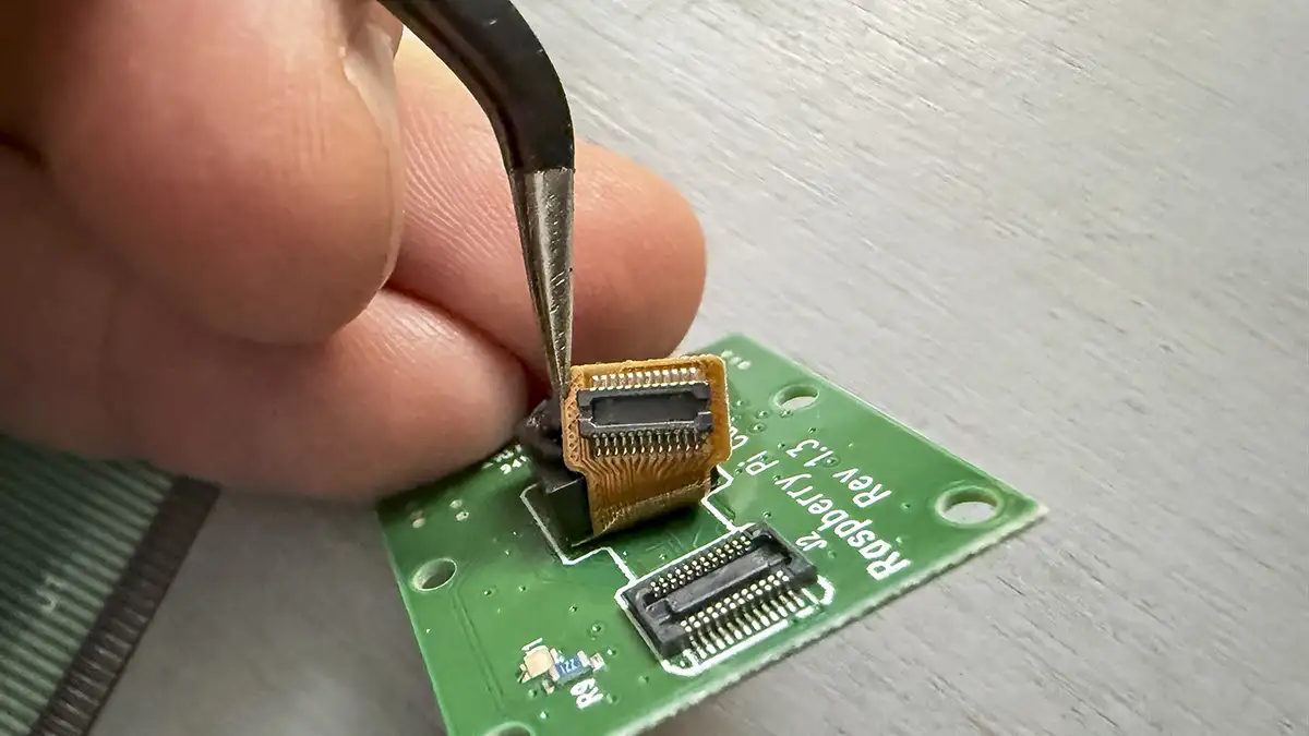
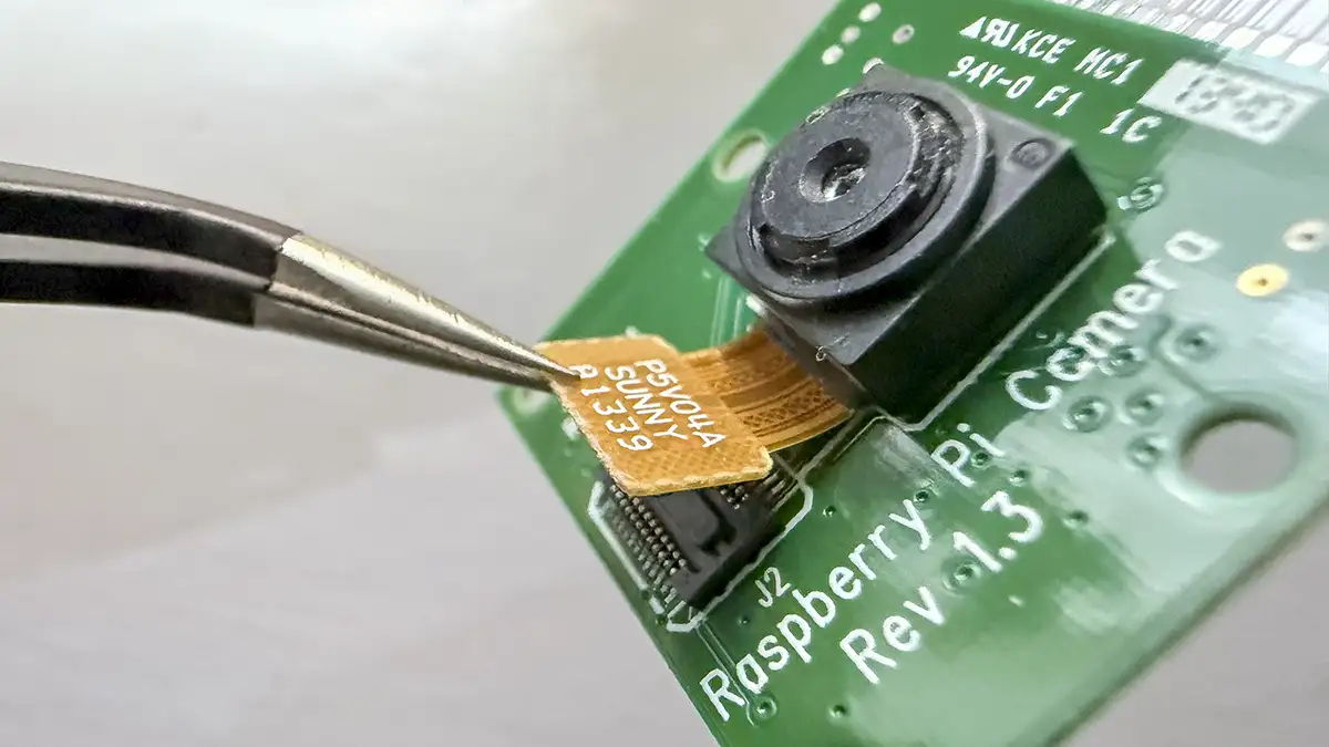
Today, FPCBs are widely used in peripheral systems mounted on moving parts of electronic products, such as displays, cameras, antennas, sensors, and keyboards. In most cases, a small functional module connects to the main assembly with the motherboard. FPCBs are ideal for these scenarios because they replace traditional cabling and significantly reduce the number of required connectors on the smaller module, allowing for a truly minimalist design.
One example from our own portfolio is a neckband earphone project we completed several years ago for a leading wearable manufacturer. The design required five PCBs—four rigid and one flexible—packed into an extremely tight enclosure. The FPCB was essential for connecting the boards while meeting strict constraints on space, track width, and signal integrity. While some technical details may have evolved since then, the project remains a solid illustration of why FPCBs demand close collaboration between electrical and mechanical teams from day one.
Many innovations are taking place with FPCBs—one of those is using conductive carbon paste rather than the usual copper foil to make traces. What are the pros and cons of that particular innovation?
Carbon paste is significantly more cost-effective than copper foil and can be applied directly to a flexible substrate using screen printing or inkjet printing. This process reduces or eliminates the need for copper etching and plating, which are energy-intensive and generate chemical waste. Carbon traces also provide excellent flexibility; they are less prone to cracking under repeated bending than thin copper, which can experience fatigue or delamination. Additionally, carbon does not oxidize like copper, making it more reliable in humid or corrosive environments.
On the other hand, carbon paste is much less conductive than copper. Creating vias or multilayer structures with carbon is more challenging, and its higher electrical resistance limits its use to low-current, low-frequency applications such as sensors or touch interfaces.
In short, carbon-based FPCBs complement rather than replace copper-based designs. They excel when cost, flexibility, and environmental benefits outweigh the need for high conductivity or power capacity.
Do you know of any other recent or upcoming innovations in FPCBs that could be game changers?
Yes. One promising area is the development of ultra-thin substrates and adhesive-less lamination. Some manufacturers are pushing polyimide (PI) and similar materials down to extremely thin profiles—around 2–5 µm—and pairing them with very thin metal foils such as rolled copper. Adhesive-less lamination, which bonds layers directly without glue films, can further reduce total stack thickness.
Embedded components have also been discussed for years. They remain a specialized enhancement, much like carbon-based technologies, offering key advantages in specific applications while still facing practical limitations.
For these reasons, I believe the true game changer will be hybrid PCBs combined with manufacturers’ ability to integrate multiple new technologies in a flexible, adaptive way. This approach allows designers to use the strengths of each technology, offset their limitations, and achieve cost-effective, high-quality solutions. That said, fully realizing this potential remains a significant ongoing challenge.
Is FPCB the right fit for your project?
Flexible PCB design is not just about bending circuits—it's about rethinking the entire development process. Success requires early collaboration between electrical, mechanical, and industrial design teams, careful material and supplier selection, and a realistic understanding of what flexibility adds in terms of both opportunity and complexity.
At Consilia, we've been helping customers navigate these challenges across a wide range of industries, from wearables to industrial applications.
Ready to discuss your next project? Get in touch.
Interesting external resources


Case studies
Related Consilia projects

Neckband Earphones for Hearing Protection
The task was to design a new wearable product fitting into an existing family of high-end headphones for hearing protection. Read more in our case study.